IBM claims that, in partnership with Samsung, it has made a breakthrough in semiconductor design. It says Vertical-Transport Nanosheet Field Effect Transistor (VTFET) technology could “help keep Moore’s Law alive for years to come.” Teasing its advanced semiconductor design, IBM asserts that VTFET can produce chips with double the performance or up to 85 per cent greater power efficiency than FinFET alternatives.
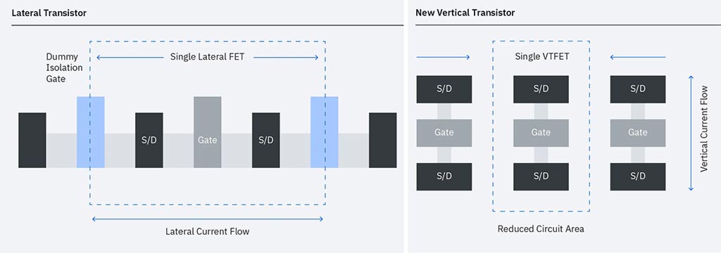
In current traditional chip designs the transistors are arranged flat on silicon wafers, with current flowing across the surface, side to side (see diagram below left). VTFET design (diagram below right) adds a new dimension as it “layers transistors perpendicular to the silicon wafer and directs current flow vertical to the wafer surface.”
Incidentally, the new approach allows for relaxing of physical constraints on transistor gate length, spacer thickness, and contact size to more optimal values.

IBM researchers previously demonstrated scaling beyond nanosheet technology in CMOS semiconductor design and reckon that VTFET could be used “to provide two times the performance or up to 85 percent reduction in energy use compared to the scaled FinFET alternative.”
In May, IBM announced 2nm mode chip designs, delivering up to 50 billion transistors in the space of a human fingernail. VTFET with its extra dimension is claimed to dramatically improve density scaling “by shrinking the Gate Pitch and eliminating dummy isolation gates.”

Practicalities
The EETimes notes that IBM/Samsung aren’t alone in developing vertically-stacked transistor and nanochip designs. Intel and TSMC have research going down similar avenues, to progress density as we scale down to the Ångstrom era. Last but not least, IBM/Samsung didn’t provide any guidance with regard to the VTFET timeline, so it is hard to see when/if such transistor designs will make it to commercial production. It has created test chips using VTFETs, ahead of this announcement, though.

