
Samsung has started mass production on its new 3nm process node using, for the first time ever, MBCFET Gate-All-Around (GAA) transistor architecture.
The tech giant touts the new 3nm process node as its most advanced chip production technology yet, allowing for smaller, densely-packed chips with increased performance and efficiency. It promises a marginal increase in performance compared to the 5nm predecessor, claiming reduced power usage of up to 45 per cent, performance uptick of 23 per cent, and a reduced surface area of 16 per cent.
Analysis
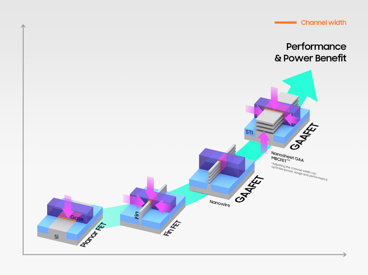
Multi-Bridge-Channel FET (MBCFET) is Samsung’s new GAA transistor architecture that allows for wider channels in gates for electricity to flow through, offering a reduction in voltage levels when compared to previous FinFET transistor architecture.
As the name implies, the Gate-All-Around translates to the channels being surrounded by gates allowing for more drive current to pass through, therefore foregoing previous performance limitations of FinFET, which only used three sides. Samsung also claims this provides opportunity to be its most flexible design yet, allowing for easy channel width adjustments to meet customer’s needs.
For now, the first generation of 3nm chips are currently designed for high-performance, low-power computer applications, with plans to transition the node in use with mobile processors. Additionally, a second-generation 3nm process is also in the works, with the goal of further reducing power consumption by up to 50 per cent, improve performance by 30 per cent, and a reduced surface area of 35 per cent when compared to the current 5nm process node.

“Samsung has grown rapidly as we continue to demonstrate leadership in applying next-generation technologies to manufacturing, such as foundry industry’s first High-K Metal Gate, FinFET, as well as EUV. We seek to continue this leadership with the world’s first 3nm process with the MBCFET™,” said Dr. Siyoung Choi, President and Head of Foundry Business at Samsung Electronics.
“We will continue active innovation in competitive technology development and build processes that help expedite achieving maturity of technology.”
Suffice to say, the new 3nm process node is a welcome addition, seeing as rivals and world’s largest foundry, TSMC, is also ramping up production of its own 3N process. And since the new technology will soon be implemented in mobile applications, it would be interesting to see how the technology melds with upcoming Exynos chips.