
Intel Foundry has just given us an update on the new subset of its 18A chip manufacturing process, dubbed 18A-P, which the company says can increase performance by up to 9% compared to 18A, while using the same amount of power. In addition, Intel says the enhanced node offers superior thermal properties to 18A, and that it maintains full backward compatibility with existing 18A IP.
Intel unveiled the details at the 2026 VLSI Symposium in Hawaii, and says that 18A-P is now in what it calls “risk production.” This basically means Intel hasn’t completed the official qualification process on this node, but that it’s confident enough in the data it’s seen that it can start ramping production with a view to selling the dies produced on it.
More performance, less power
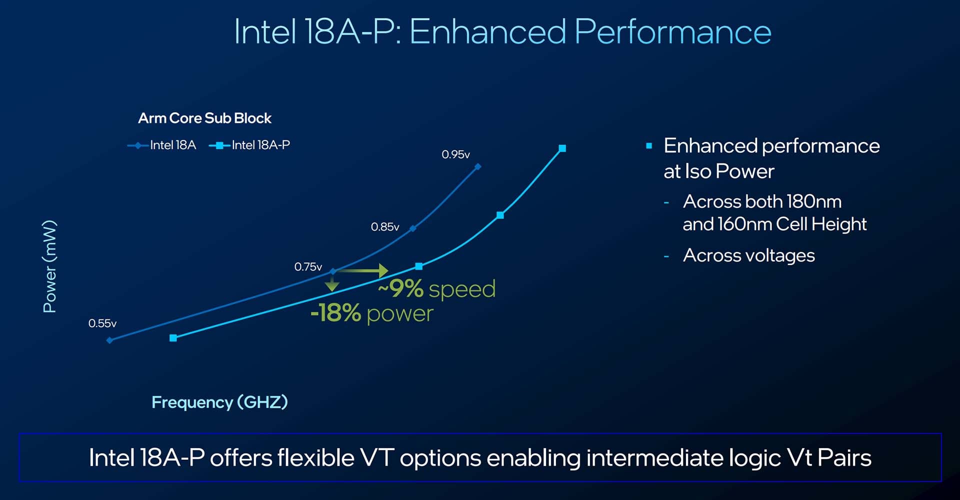
Demonstrating the potential performance on offer, Intel gave an example of two identical Arm core sub-blocks, one produced on 18A and one on 18A-P. According to Intel’s data, when you plot the frequency against the power of both chips, it shows improved performance for the same or less power on 18A-P. In simple terms, Intel says you could have the same frequency while using 18% less power, or you could improve clock speed by 9%, while maintaining the same power level. That’s a big deal for wattage-constrained devices.
Speaking to the press in advance of the announcement, Intel Foundry vice president, Chris Auth, claimed that you’ll see similar results to this Arm sub-block across the board. “You can look at other circuit designs,” says Auth, “and you’ll see a very similar type of values for either speed or power that you get on that circuit design.”
Power Boost
One of the ways Intel is improving performance is with a new dual-contact design that it calls Power Boost. It’s designed to increase drive current through the transistor, meaning you can achieve higher frequencies at the same level of capacitance.
You can see the principle outlined in the image of a four-channel RibbonFET 18A-P transistor on the right below, where there are now two contacts – on the front side and back side – rather than just one on the front, as with 18A. As a refresher, Intel moved to backside power delivery with 18A – in very simple terms, this means power is supplied to the back of the transistor, so it doesn’t interfere with all the signal lines on the front side.
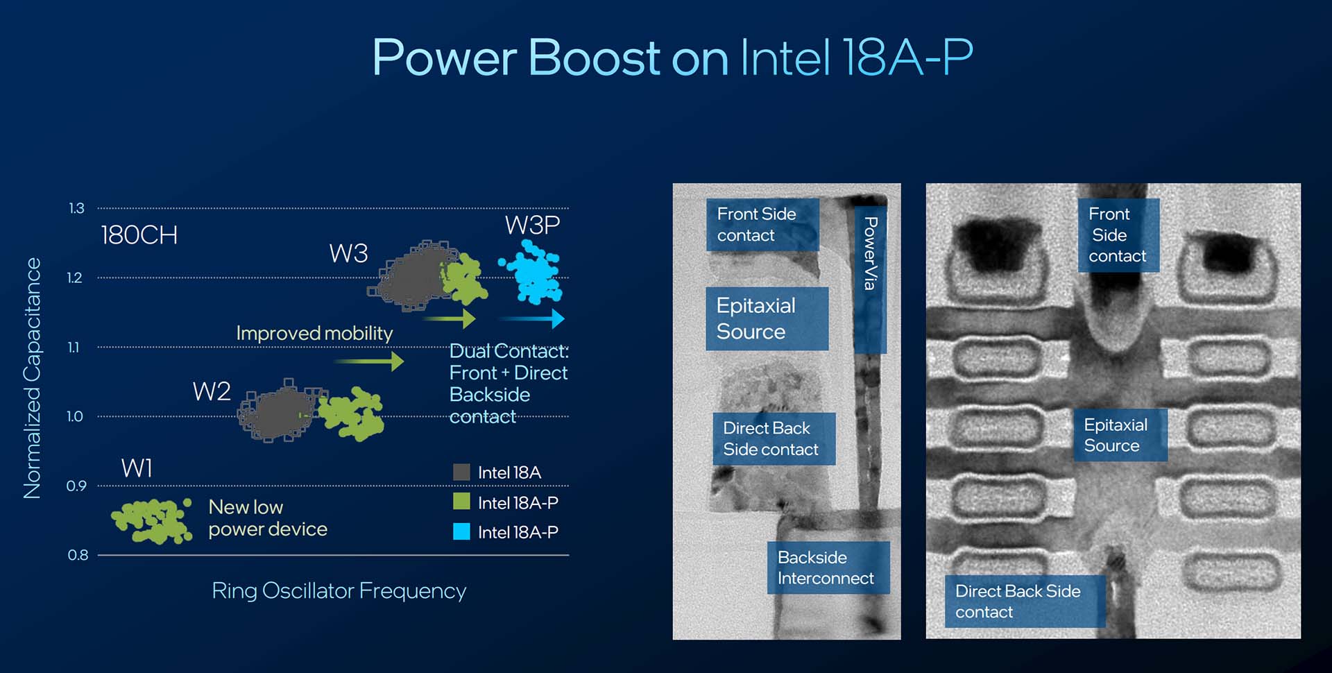
Auth provided the analogy of a crowded theatre to explain how this works. “If you look at where 18A is, all of this current that you get has to converge and go in through this front side contact, and that causes a lot of crowding. It’s very similar to if you’re at an auditorium, and everybody has got to go through one door, all these rows of the theatre go in, and they all have to funnel through.
“It becomes really crowded. There’s a bottleneck. So what you really want is another door where people can leave. And that’s what we’ve done, we’ve added this direct backside contact here, and that’s enabled by having backside interconnects.”
Improved thermals
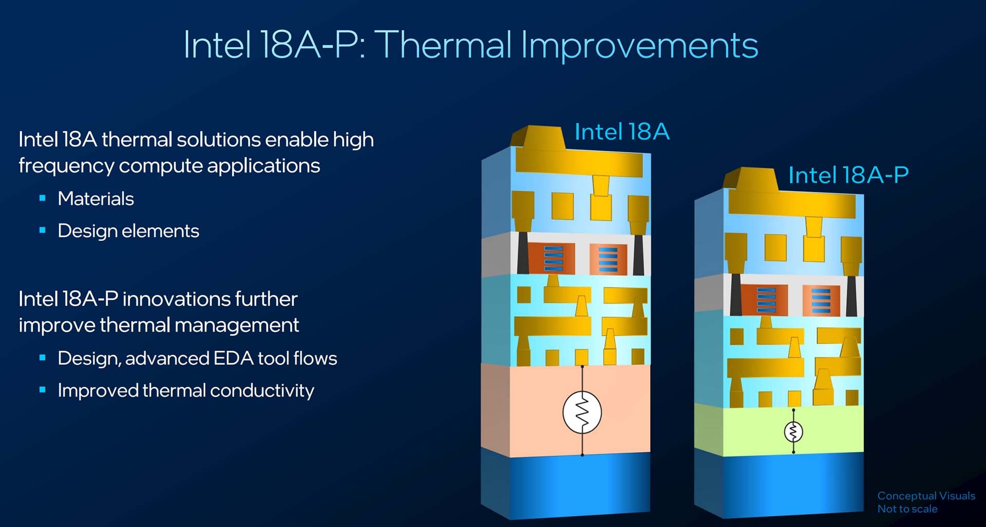
Intel also claims that thermal resistance has been improved by 20-40% on 18A-P compared to 18A. This is down to a reduction in the thickness of the wafer area devoted to handling thermals, as well as moving to a new material for this section.
In addition, Intel says it’s implemented new electronic design automation (EDO) tool flows to work out where heat needs managing. “It’s thermally aware,” explained Auth, “so where there is heat, it adds in a more extensive interconnect or vias, in order to move that heat very quickly out towards the substrate where it can dissipate away.”
As a final tease, Intel gave us some hints of future developments in the works. These include using ruthenium as an interconnect, rather than copper, which it says offers 35% capacitance reduction. Intel is also demonstrating a monolithic complementary FET (CFET) tech inverter, which vertically stacks NMOS and PMOS devices at a 45nm gate pitch. Intel describes CFET tech as the “next anticipated major shift for continued logic scaling,” enabling chip companies to build upwards with different materials.