
The 67th IEEE International Electron Devices Meeting 2021 kicked off this past weekend, and it will continue to be a source of cutting-edge electronics announcements until Wednesday. PC processors giant Intel has made a splash at the event with a presentation regarding its “relentless pursuit of Moore’s Law.” Reading on, you will find out about three key breakthroughs by Intel and its partners, which will hopefully assure you that its IEDM presentation isn’t just hot air or wishful thinking.

Advances in scaling technologies
Intel has conducted considerable R&D in scaling technologies for delivering denser transistor structures in future products. You will have already heard of Foveros next-gen advanced packaging for tiled microprocessors. Foveros Direct will supersede this tech, bringing denser, and more flexible integration of processing tiles on a chip. “Instead of using solder connections, which slow down data transfer, Foveros Direct implements direct copper-to-copper connections that result in lower latency and higher bandwidth while reducing die area required for communication,” explains Intel in the video below.
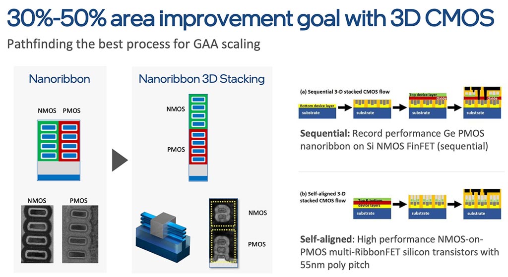
In its vision of the coming post-FinFET era, Intel sees an approach to stacking multiple (CMOS) transistors that aims to achieve a maximized 30-to-50 per cent logic scaling improvements. In the video below, Intel Component Research Engineer, Marko Radosavljevic, uses augmented reality to talk to you about the transition from FinFET (2011) to RibbonFET (coming with Intel 20A), and beyond thanks to transistor-stacking technologies. Intel is currently testing various silicon-on-silicon stacking techniques but is favouring “self-aligned” processes.
Last but not least, with a view towards improved scaling, Intel is looking carefully at novel and 2D materials to overcome silicon-based limits beyond 2025.
Bringing new capabilities to silicon
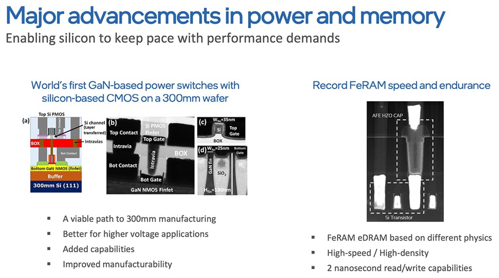
Intel also recognises the importance of high-speed power delivery for CPUs. It has already advanced to create “the world’s first integration of GaN-based power switches with silicon-based CMOS on a 300 mm wafer,” for low-loss on-chip power, reducing motherboard complexity and PCM space.
Next-generation embedded DRAM technology, with low-latency read/write capabilities, is being investigated. Intel is researching novel ferroelectric materials to try and crack the problem of huge memory demands by all sorts of tasks from AI to gaming.
Silicon transistor-based quantum computing,
Often we read about the extraordinary capabilities already delivered by quantum computers, and the massive potential that is clear to see on the path forward. Intel has wisely put resources into melding its silicon tech such as CMOS manufacturing, with quantum computing.
Previously, Intel showcased full 300 mm qubit process flows for scalable quantum computing. It is known that Intel and IMEC are making progress with spintronic materials research. Perhaps most importantly, though, at IEDM 2021, Intel demonstrated “the world’s first experimental realisation of a magnetoelectric spin-orbit (MESO) logic device at room temperature.” The demo shows the potential of a new type of switching nanoscale magnet transistor, says Intel.
Later today, Club386 will be looking at what Intel and ASML see as the future manufacturing technology which will take us/them beyond EUV. Please stay tuned.