
The following article is sponsored by AMD. Any opinions expressed are my own.
Introduction
Worth $175 billion at the time of writing, Advanced Micro Devices, or AMD to you and me, was founded on May 1, 1969. The company was formed by Jerry Sanders and several colleagues who all previously worked at Fairchild Semiconductor.
The Am9300 shift register was the first product to be built by AMD in 1970. The same year saw the company build its first proprietary product, the Am2501 logic counter, which was considered a commercial success.
Part of AMD’s early appeal was guaranteeing the robustness of its chips to US Military Standard, which most competitors were not able to do; chip failure was more common in the early days of semiconductor engineering and manufacturing.
Moving through the next decade, AMD created the world’s first 512K EPROM in 1984 and first 1M EPROM in 1986. By their programmable and data-retention nature when switched off, EPROMs enabled customers to accelerate the prototyping of products.
“Readers of a certain vintage will remember the emergence of AMD’s Athlon range of processors in 1999”
1991 marked an important watershed in AMD’s history as it debuted the AM386 family of in-house-designed processors which sold in millions of units and made the firm a genuine competitor in the consumer CPU space. If you wondered where the numerical part of our website’s name comes from, look no further than storied CPU history.
I have fond memories of this time as the CPU wars of the 90s sparked my interest in all things related to PCs. Perusing the tightly-packed sheets of the Micro Mart magazine, scouring for bargains, and then heading over to computer fairs – usually and strangely held at horse racecourses – and dimly-lit stores still evokes pangs of nostalgia.
Readers of a certain vintage will remember the emergence of AMD’s Athlon range of processors in 1999. The release was important for AMD’s image and bottom line as the seventh-generation processors outmuscled the competition in many areas. Athlon become the first x86-based desktop processor to run at a 1GHz clock rate and was duly named Athlon 1000.
Such a seminal number prompted me to raid the squirreled cash jar and purchase 1,000MHz of Thunderbird processing power. Though it was a single-core, single-thread chip – how quaint any tech-savvy teenager would now say – the chip was a source of pride and peer envy in equal measure.
64-bit pioneer
AMD pioneered 64-bit x86 computing in 2003 by releasing server-orientated Opteron 64 and desktop Athlon 64 models and followed these innovations by launching the world’s first x86 dual-core processor in 2004 and native quad-core in 2008.
Looking to exploit the advantages of CPU and nascent GPU computing, AMD purchased graphics specialist ATI in 2006 for $5.4bn. That seemed like an incredible outlay at the time, and I remember reporting upon it with minor disbelief, but now these sums barely make the page on financial journals.
By 2008, AMD had spun-off its manufacturing division by partnering with an investment company formed by the government of Abu Dhabi. The resulting manufacturing firm came to be known as GlobalFoundries. I’d say the move was dictated by financial considerations rather than long-term vision, no matter what the public line.
Using the combined skills of its CPU and GPU teams, AMD launched the first true hybrid processor which amalgamated the benefits of both types of compute into a single chip. Redefined as an Accelerated Processing Unit (APU), at that time it provided AMD with a unique performance advantage over the CPU-only competition.
I recall AMD having some difficulty in making enough APUs to satiate demand, and I heard first-hand from a reliable source that wafers of first-generation Llano APUs were hand-carried through GlobalFoundries’ Dresden fabrication facility. There’s nothing like old-fashioned elbow grease juxtaposed alongside cutting-edge manufacturing measured in the nanometres, right?
The calm of Zen born from the chaos of Bulldozer
Most commentators, including myself, remember AMD’s PR machine previously having to work overtime in convincing the tech press that previous-generation Bulldozer, and subsequent iterations, were solid alternatives to the strong incumbent competition. The truth was they weren’t, because the clustered multithreading technology was mired in inefficiency.
“I believe Zen was only possible due to the lacklustre reception to Bulldozer CPUs”
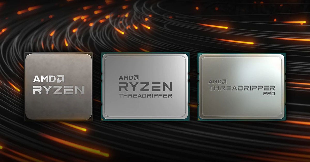
AMD really hit the straps with the Zen architecture which debuted in 2017 and was productised as Epyc for the server/workstation market and Ryzen on desktop and laptops.
A number of notable firsts emanated from the design, including the industry’s first 16-core high-end desktop processor (Ryzen Threadripper), the highest-performing 8-core processor (Ryzen), and fastest processor for thin-and-light laptops (Ryzen Mobile).
I believe Zen was only possible due to the lacklustre reception to Bulldozer CPUs, forcing AMD to adopt a clean-sheet design and build a new architecture without the shackles imposed by, in hindsight, poor legacy decisions. Zen’s reach was far-sighted, too, as the modular nature of the chiplet design enabled AMD to launch products simply not economically possible with established monolithic implementations. From the chaos of Bulldozer came the calm of Zen.
Since then, AMD has further introduced the first 16-core gaming chip (Ryzen 3950X), the first 64-core x86 server processor (Epyc 7002), and the first CPUs and GPUs to be built on the energy- and space-saving 7nm manufacturing process. The very latest chips use the Zen 3 architecture for best-in-class performance across a number of workloads and segments.
Ryzen and Epyc processors turned around AMD’s fortunes both externally and internally. I’ve noticed a sea change in ambition, confidence and scope from long-standing employees who previously had to defend, let’s be candid, inferior products. Now, AMD doesn’t frame itself in the shadow of others, and roadmap execution isn’t a kneejerk reaction to what competitors are releasing in this quarter. It’s certainly no coincidence that AMD’s fortunes have rallied since present CEO, Lisa Su, took the reins in 2014. I’ve had the pleasure of speaking with her on numerous occasions, and she remains as affable and forthcoming now as when she first took on the job.
A clear path to AI
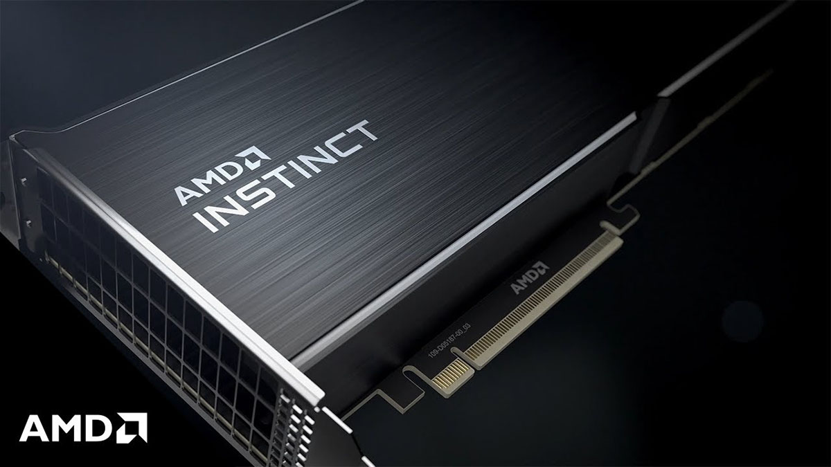
Moving to the very present, AMD introduced the Radeon Instinct MI200 series accelerators. Purposely built for speeding up complex research programs run in the high-performance computing (HPC) space, and founded on the latest CDNA 2.0 architecture, the dual-die accelerators, connected via high-speed Infinity Fabric, pack in an incredible 58bn transistors. Backed by 128GB of HBM2E memory, the MI250X offers 47.9TFLOPs of double-precision compute and 383TFLOPs of half-precision throughput.
From my view, AMD wants to target growth areas in which it previously had only a sliver of a foothold. The world of AI demands incredible heterogenous compute power – supercomputers are primed for it – and AMD believes its portfolio of accelerators and accompanying software makes a strong case for adoption. From where I sit, it’s becoming more difficult to disagree with that assertion, but this confidence in execution is tempered by the knowledge that competitors are also putting tremendous hardware and software resource in the same place. The future of AI computation is a prize well worth fighting for.
To whit, along with the latest Epyc server processors, Radeon Instinct MI200 accelerators feature in Oak Ridge National Laboratory’s Frontier exascale computer, which is expected to deliver more than 1.5 exaflops of peak computing power – over 3x the performance of the fastest supercomputer on record today, the Fugaku, and about 10x faster than the Oak Ridge’s Summit supercomputer from 2018. Quite a feat considering Summit remains to this day the speediest supercomputer in the USA.
3D V-Cache coming to a Ryzen and Epyc near you
The near-future ambitions of AMD build on the work of recent years. The company is set to invigorate the present Ryzen line-up by equipping the next generation with what the company terms 3D V-Cache. Though based on the existing Zen 3 architecture available on Ryzen 5000 series, AMD massively boosts the refreshed chips’ pool of L3 cache by using a novel technique whereby an extra 64MB of cache is stacked vertically on each chiplet.
“AMD cites gaming as a good example of 3D V-Cache deployment”
Shown on a prototype Ryzen 9 5900X during CES 2021, adding an extra 128MB of L3 – across two chiplets – triples the amount available on the regular, non-3D V-Cache chip.
Having more on-chip cache is beneficial because it is an order of magnitude faster than accessing the same information held in system memory or, as a last resort, computer storage. Latest-generation Radeon GPUs also have more-than-usual cache for the same underlying reasons, known by the catchy name of Infinity Cache.
Suffusing next-gen Ryzens with 3x the L3 cache plays particularly well in applications that are more sensitive to memory bandwidth and location proximity to the compute cores. AMD cites gaming as a good example of 3D V-Cache deployment, offering up to 15 per cent higher gaming performance at 1080p when compared directly against an otherwise identical Ryzen processor without this modern technology.
Presented in the familiar AM4 form factor and requiring no software intervention to function at optimum levels, 3D V-Cache-equipped Ryzens are due in Q1 2022. We won’t have long to wait to verify AMD’s performance-enhancing claims.
AMD is using the same 3D V-Cache technology on server- and workstation-optimised Epyc processors. The current third-generation Epyc processors, codenamed Milan, are to be supplemented in early 2022 with L3 cache-injected models known as Milan-X.
Current Epyc 7003 series chips top out at an impressive 256MB of L3 cache per processor, split 16MB over 16 CCXes. Through stacking extra cache vertically – or 3D, if you will – AMD is also able to triple the amount of L3, to a total 768MB per top-bin chip. In a 2P dual-processor solution, common in the industry, this equates to a whopping 1.5GB of L3 per motherboard.
I feel it’s vitally important companies strive to innovate outside the known process and pure architecture box that has been the development handbook for years. These two drivers naturally offer an uplift from one generation to the next, but there will come a time when large advances for both become harder to come by. It’s then that mid-term updates such as V-Cache make the most sense. Engineering has to be cutting edge and smart at the same time.
In the fast-moving world of technology, AMD continues to innovate at pace with plenty more to come in 2022.