

The most complex and largest chips AMD has ever created are the datacentre-optimised Instinct MI300 family. Announced last year and primed to take centre stage in the upcoming El Capitan supercomputer, AMD now takes the architectural wraps off. If you like huge numbers, clever packaging, and impressive engineering, the chiplet-infused Instinct MI300 family are absolute beasts. They’re important for AMD’s continuing bottom line, too, as grabbing a larger slice of the lucrative and ever-expanding datacentre AI pie is a serious priority.
The family arrives in two distinct flavours. There’s the 13-chiplet MI300A using a whopping 146bn-transistor design that houses 24 Epyc 4th Generation CPU cores, CDNA 3 graphics, and multi-stack 128GB of HBM3 memory. Appreciating much of generative AI processing works best solely on GPUs, the 153bn-transistor MI300X shelves the three-chiplet Epyc portion and devotes all resources to GPU compute via two further graphics chiplets.
High-performance silicon
Furthermore, MI300X increases HBM3 memory to 192GB per chip, which is enough to fit large-language models such as Falcon-40B – a 40-billion parameter model – on a single GPU accelerator. This larger memory footprint is viewed as a key advantage over Nvidia, where fewer AMD accelerators are needed to handle a set-sized LLM inference workload. In fact, a single MI300X runs models with up to 80-billion parameters. Large enough to accommodate the biggest Llama 2 parameters.
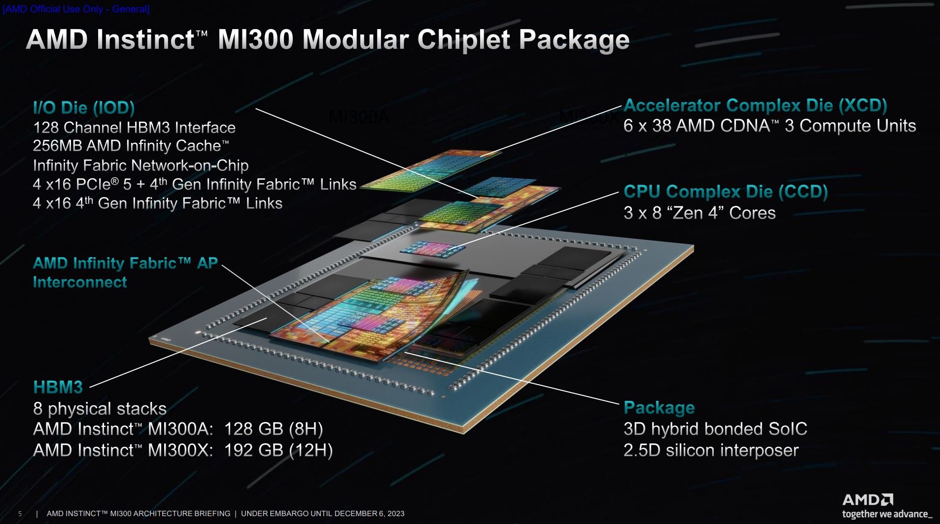
Let’s look under the hood of HPC-geared MI300 first. Cutting to the quick, the 6nm I/O Dies (IOD) are the beating heart of the chiplet package. Unlike regular server processors and speaking to the complexity of this chip, there are four IODs per package, connected to each other via a new technology known as Infinity Fabric AP. Necessary to boost internal and external bandwidth, they combine to process 128 channels of HBM3 memory throughput. Pulling something from consumer graphics, this generation of Instinct also uses bandwidth- and power-saving Infinity Cache.
Talking of memory, eight 16GB stacks of HBM3 lead to a total 128GB. AMD divvies up connection such that two-stack multiples connect to one IOD via a 32-channel interface. The same is true for MI300X, actually, though each stack carries 50% more capacity.
Scale is an important watchword. These chips are designed to be connected together to form large nodes – the El Capitan supercomputer is an extreme example of this philosophy – so there are 64 Infinity Fabric lanes on each processor. Furthermore, 64 PCIe 5.0 lanes provide expansion opportunities for specific accelerators.
Modular CDNA 3
Packaging complexity must have caused AMD serious headaches as bringing together multiple technologies, on different nodes, is no mean feat. Though the 24-core Epyc portion of MI300A uses the same ISA as widespread server processors, the way in which it connects to the package is altogether different. 3D hybrid bonding replaces traditional global memory interconnect links. Another necessary difference is addressing space, reduced from 57 bits on standalone Epyc to 48 bits here, and the reason for doing so is continuity with the GPU.
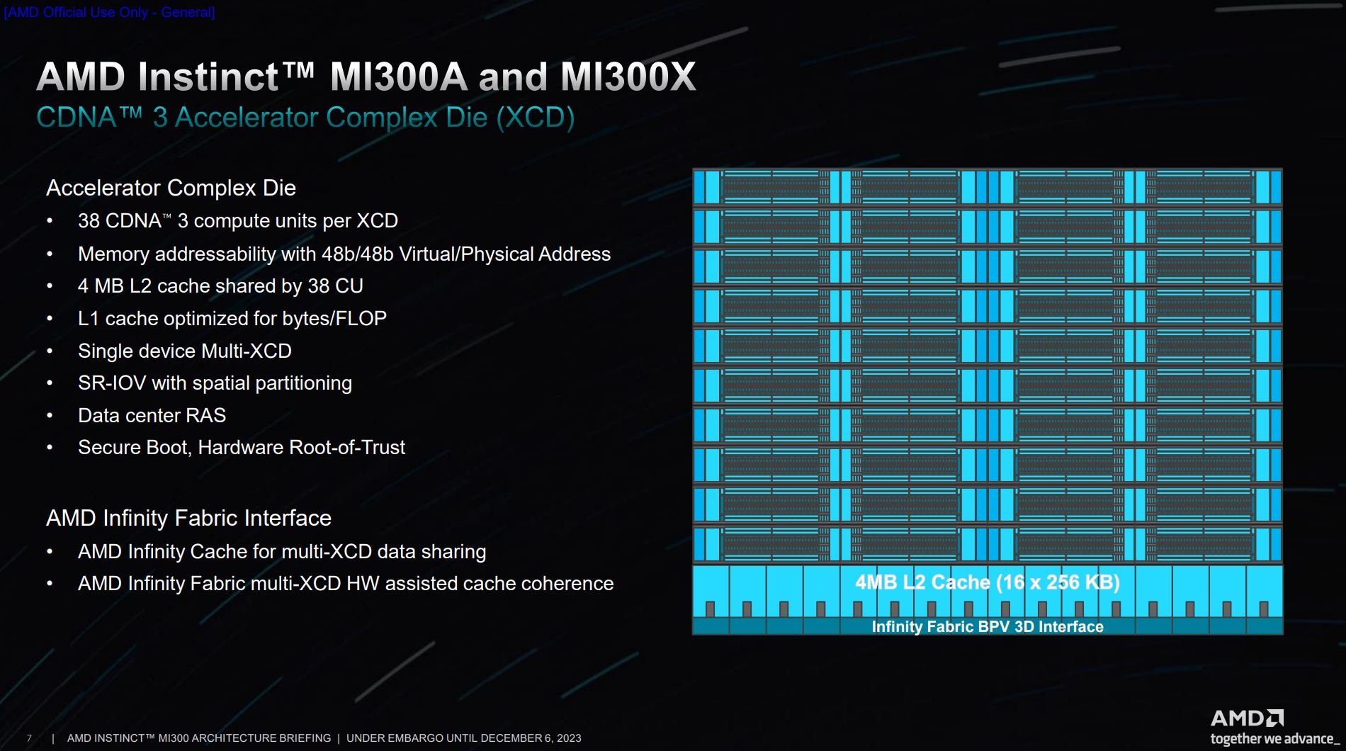
Getting to the meat of the chips, MI300 represents the first time AMD splits the Compute Units into chiplets, much in the same way the latest consumer graphics cards tackle the problem of shoehorning more performance with reasonable cost. Recall, if you will, the prior Instinct MI2xx generation used a monolithic approach.
This time around, scale again enforces the change to the 5nm Accelerator Complex Die (XCD) units. AMD activates 38 out of a possible 40 Compute Units per XCD, with the remaining two left untapped due to, I imagine, yield and cost considerations. The idea is that multiple XCDs work in tandem and present to workloads as a monolithic die. Of course, this approach requires top-notch scheduling amongst dies, but AMD has already demonstrated this expertise capability on the consumer Radeon RX 7900 Series.
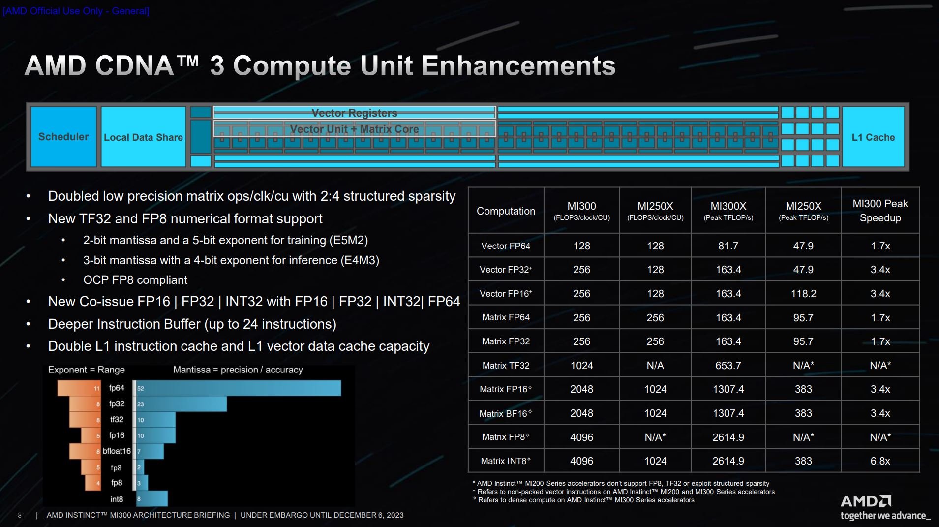
Considering emerging workloads, the CDNA 3 architecture brings support for two numerical formats known as AI-optimised TensorFloat TF32 and FP8. The hybrid TF32, in particular, has the same range as traditional FP32 and the same precision as today’s FP16. The end result is a significant speed-up – the to tune of 6x – for machine learning frameworks when compared to running the more intensive FP32 alone.
There’s also capability to co-issue certain instructions for greater throughput, and it’s one reason why there’s a greater-than-expected uplift over the last generation in corner-case scenarios.
Tying it together
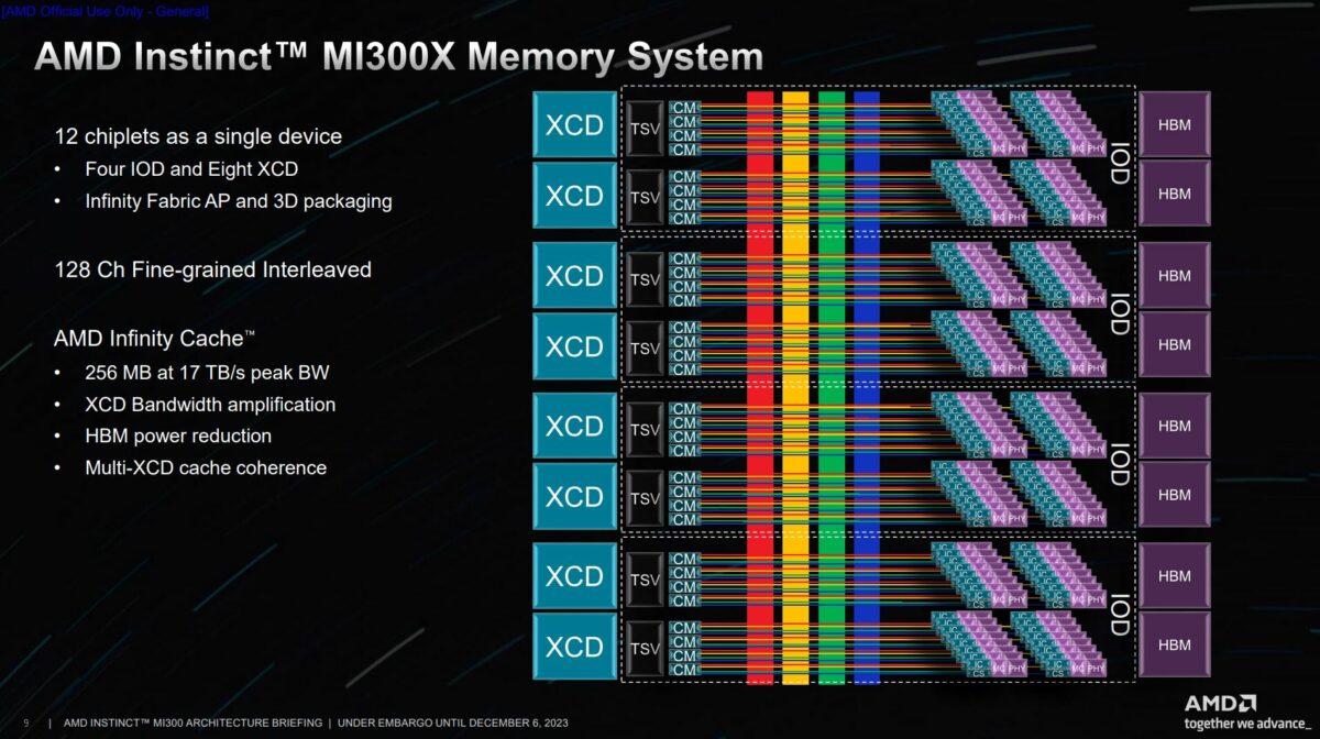
So how does this all fit together? Good question. Remember that the MI300X is a 12-chiplet single-APU design. Breaking it down, all resources are geared towards GPU XCDs. Two 38CU XCDs and two HBM stacks each connect to one of the four IODs. Keeping consistency across the various facets, recall that each HBM3 stack connects via a 16-channel interface. The same is true of an XCD, which also uses 16 channels, meaning one XCD can privately communicate with one HBM stack, though their bandwidth levels are not the same, as I’ll explain below.
Of course, no XCD or HBM stack is an island. Intra-chip communication is handled by Infinity Fabric AP links such that data or workload on any part of the chip can be accessed elsewhere. For example, the top-left XCD can jump over the IF and grab the contents of the bottom-right HBM stack through IOD traversal.
Look more closely to reveal where the all-new Infinity Cache resides. Represented by green rectangles and situated before the memory controller, it’s no surprise the peak bandwidth of the Infinity Cache matches the peak bandwidth of the XCDs, noted at 17TB/s.
In sum, MI300X is home to 304 Compute Units, 128-channel memory interface to 192GB of HBM3 memory, and 256MB of Infinity Cache.
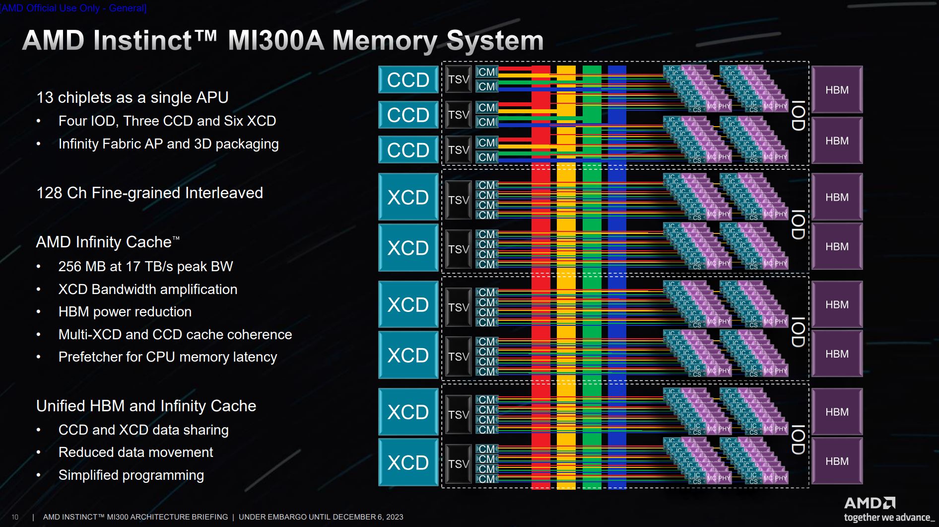
Switching gears to hybrid MI300A, the two topmost XCDs are replaced by the three-CCD Epyc CPU also built on a 5nm process. Everything else stays the same, other than HBM3 memory dropping from 192GB to 128GB. Sounding trivial at first glance, AMD engineered enough space on regular Epyc chips to allow for them to connect to 3D-stacked solutions like MI300 in the future.
Why chiplets make sense
Teasing it out further, it’s easy to see how AMD can switch between MI300A and MI300X production, as the chiplet change is relatively straightforward. Smart engineering. This time around, the Infinity Cache serves both the XCD and CCD and retains unified coherence between them. The upshot is cached data is shared and reduces movement that burns power unnecessarily.
Crunching the numbers, MI300A carries 228 Compute Units, 128-channel memory to 128GB of HBM3 memory, 256MB of Infinity Cache, and a 24-core Epyc-like CPU.
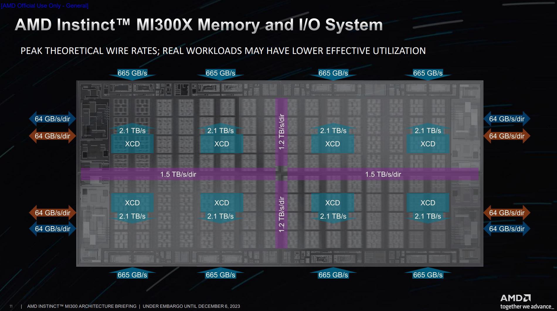
Tying the bandwidth together is this handy slide,, and you’re looking at four symmetrical IODs. Each stack of HBM3 memory operates at 5.2Gbps and produces a sum 665GB/s that feeds into the IOD. Two stacks yield around 1.3TB/s bandwidth. The XCDs, meanwhile, push out a cumulative 4.2TB/s per IOD. On the outside you see the Infinity Fabric and PCIe 5.0 speeds to either peripherals or other chips.
The purple rectangles represent the Infinity Fabric AP links that ties these four IODs together. It’s higher horizontally because there’s extra allocation for I/O traffic on top of regular memory traffic flowing between XCDs and IODs.
MI300A supports either a single partition where all six or eight XCD units work as one, or three partitions split into groups of two. MI300X, meanwhile, supports either one, two, four, or eight partitions, with an equal amount of memory allocated to each. One would consider spatial partitioning the processing units for SR-IOV operations.
Packaging problems
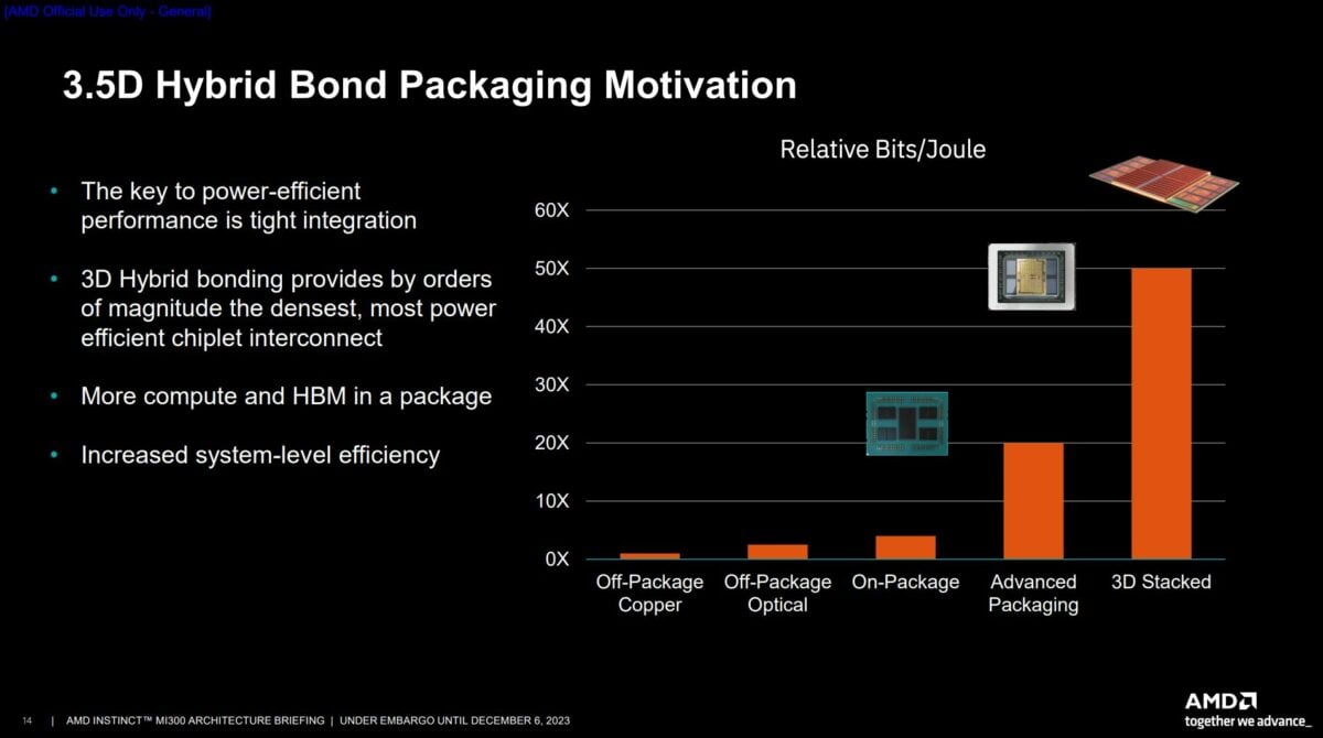
I alluded to packaging headaches earlier, and they are legion for a 13-chiplet product like MI300A. Putting so many disparate technologies together in an energy- and cost-efficient package is arguably more impressive than the individual chiplets themselves. “There’s no other way to integrate the amount of silicon, HBM, cache, compute, CPUs, and GPUs without 3D stacking,” said AMD’s Sam Naffziger.
In fact, it’s impossible MI300A/X exists in its present form without 3D stacking and associated packaging know-how, as running with traditional techniques would leave far less power headroom for the Compute Units to run at acceptable speeds.
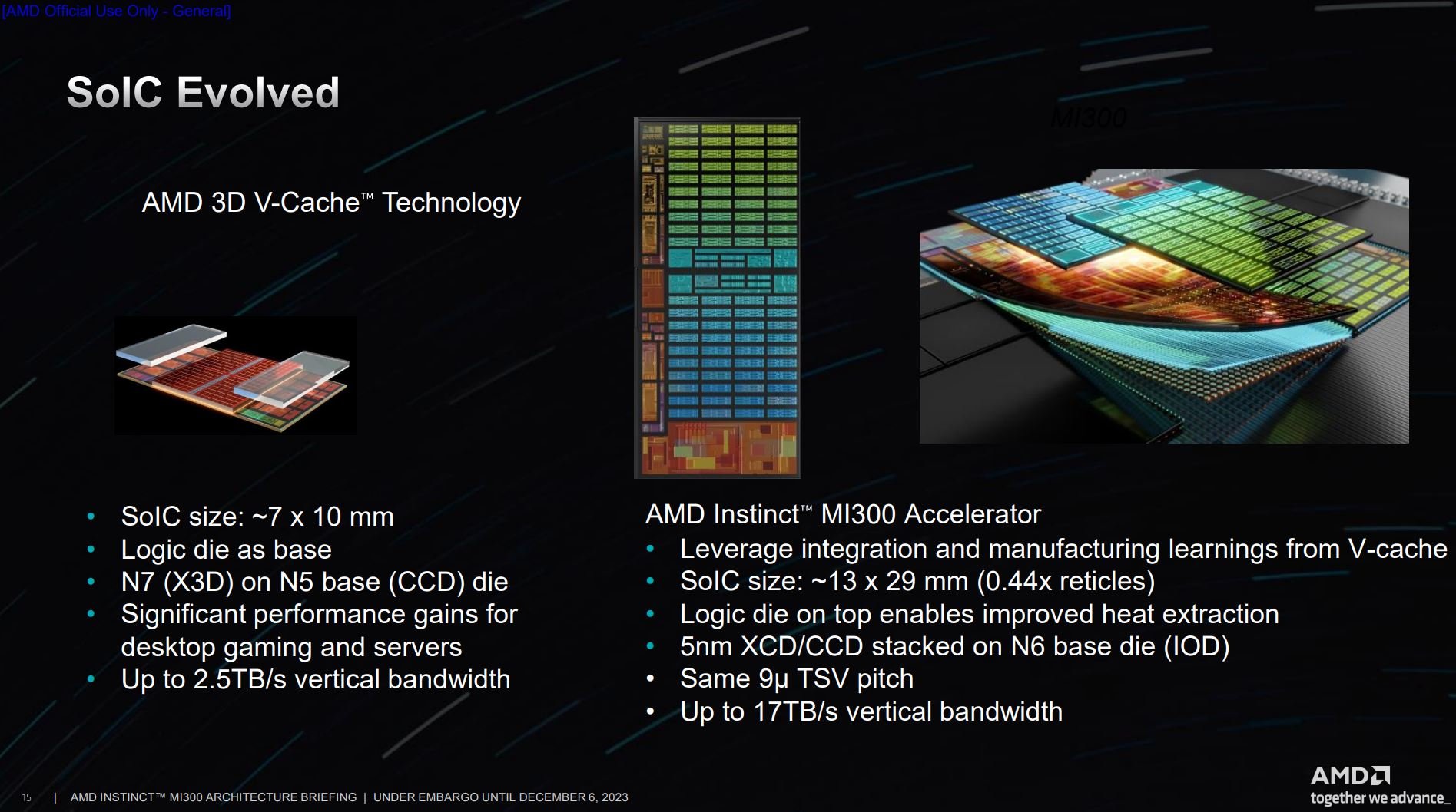
Part of MI300’s packaging existence traces its roots back to the 3D V-Cache first introduced on server Epyc and consumer Ryzen processors. The system on integrated circuit (SoIC) stacking, somewhat analogous to Intel’s Foveros, is much larger this time around, though it retains the same 9-micrometre through-silicon via pitch as 3D V-Cache.
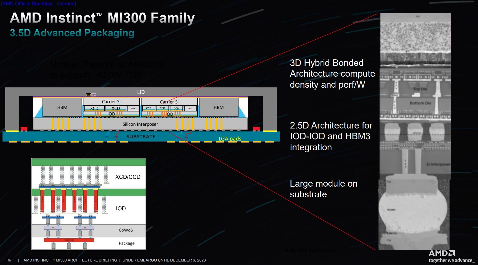
This is how a chip looks if examined from the side. The IOD dies physically sit at the bottom with either XCDs (MI300X) or a combination of XCD/CCD (MI300A) on top. On the right, you see the actual scale of each constituent part, along with the various TSVs routing through to the bumps at the bottom.
The Wrap
AMD’s MI300 line of super-processors are the culmination of many prominent technologies. Modular chiplets, expansive IODs, HBM3 memory, Epyc CPUs, improved Infinity Fabrics, and cutting-edge packaging all play a part in bringing these 100bn+ transistor behemoths to the table. They simply wouldn’t exist if any of these technologies failed to deliver upon the initial promise. Though the phrase is often bandied about, these are engineering marvels through and through.
Aside from the cutting-edge smarts, MI300A and MI300X can’t come soon enough as standalone products. Their very nature relates to high performance in HPC and AI training and inference workloads. Just how MI300X battles against Nvidia’s omnipotent H100 when running large-language models is presently unknown, but going by the specifications, signs are promising. Peering under the hood shows AMD’s latest AI-focused silicon has plenty of firepower through a forward-looking design.
Cloud providers buy at scale. If AMD can demonstrate that MI300 runs a set amount of inferencing or training with fewer instances than H100, and that they’re available sooner – reports suggest Nvidia’s best silicon has a year-long wait – there’s tremendous opportunity for MI300 to grab immediate revenue and profit.