
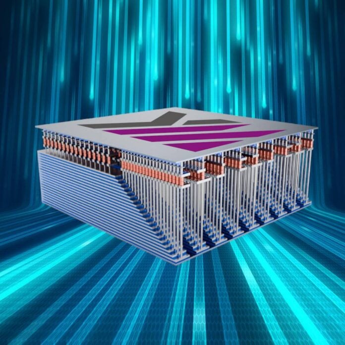
Chinese NAND flash manufacturer YMTC is apparently preparing the mass production of high-speed LPDDR5X memory. According to global tech research firm, Counterpoint Research, the company plans to build 9,600MT/s chips in its Fab 3 facility, using vertical channel transistor (VCT) 4F² cell structure technology.
Better known for its YMTC NAND flash products, it looks as though the company is now venturing into DRAM, with low-scale manufacturing apparently already in operation. Counterpoint Research claims the company has been producing about 5,000 wafers per month of its second-generation 16Gb LPDDR5X-7500 DRAM at its Fab 2 plant since October 2025. Now, it apparently plans to mass-produce LPDDR5X-9600 chips in its Fab 3 using the VTC 4F2 cell structure.
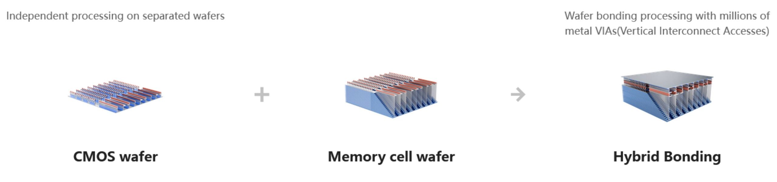
To do so, the research firm says YMTC is repurposing its proprietary Xtacking 4.0 technology, which allows it to fabricate a core memory storage array on one specialised silicon wafer, and the peripheral CMOS logic circuits on an entirely separate wafer, before combining them using hybrid bonding wafer-to-wafer stacking.
This setup would allow the firm to optimise the logic circuitry for maximum speed, 9,600MT/s in this instance, while isolating it from the intense heat generated during memory array fabrication.
Beyond wafer stacking, the other notable technology used by YMTC is the 4F² cell structure, instead of the industry-standard 6F² layout. A 4F² cell structure stands the transistor upright using vertical channel transistors (VCT), which, on paper, reduces the physical footprint of each memory cell by roughly one-third (33%) while using the exact same process node. T
That’s also without needing advanced EUV lithography machines. This is especially important for YMTC, since it can’t obtain advanced manufacturing machinery due to US export restrictions, which block it from shrinking DRAM size horizontally using smaller nodes.
Going with the 4F² cell structure is also interesting, since Micron has recently confirmed it will not bring its 4F² DRAM to market, focusing instead on the 6F² layout until 3D DRAM arrives. Micron has been working on 4F² DRAM for two decades. According to Scott DeBoer, President and Chief Technology and Products Officer at Micron, there are fundamental cost and complexity problems with 4F² scaling that ultimately will lead to 3D DRAM coming in instead.
“I can’t comment on why other suppliers would do things,” he told investors. “I can only say from our investigation of this technology over the past couple of decades, first off, it’s a bit of a myth that 4F² actually provides anything versus 6F². It’s capacitor pitch that defines the DRAM. You can build the cells, the transistors underlying in different ways, but they still have to fit under the capacitor pitch, which sets the DRAM. So some of that is just kind of smoke and mirrors in terms of talking about 4F² versus 6F².”
Whether it’s the right approach or not, it looks as though YMTC is intent on carving a spot in the DRAM market, committing a cumulative 142 billion yuan (more than 5% of sales) to research and development from 2023 to 2025, according to Counterpoint Research. In the long term, 3D DRAM will eventually supersede 6F² and 4F², but the accumulated experience in wafer bonding technology will be valuable to YMTC.