
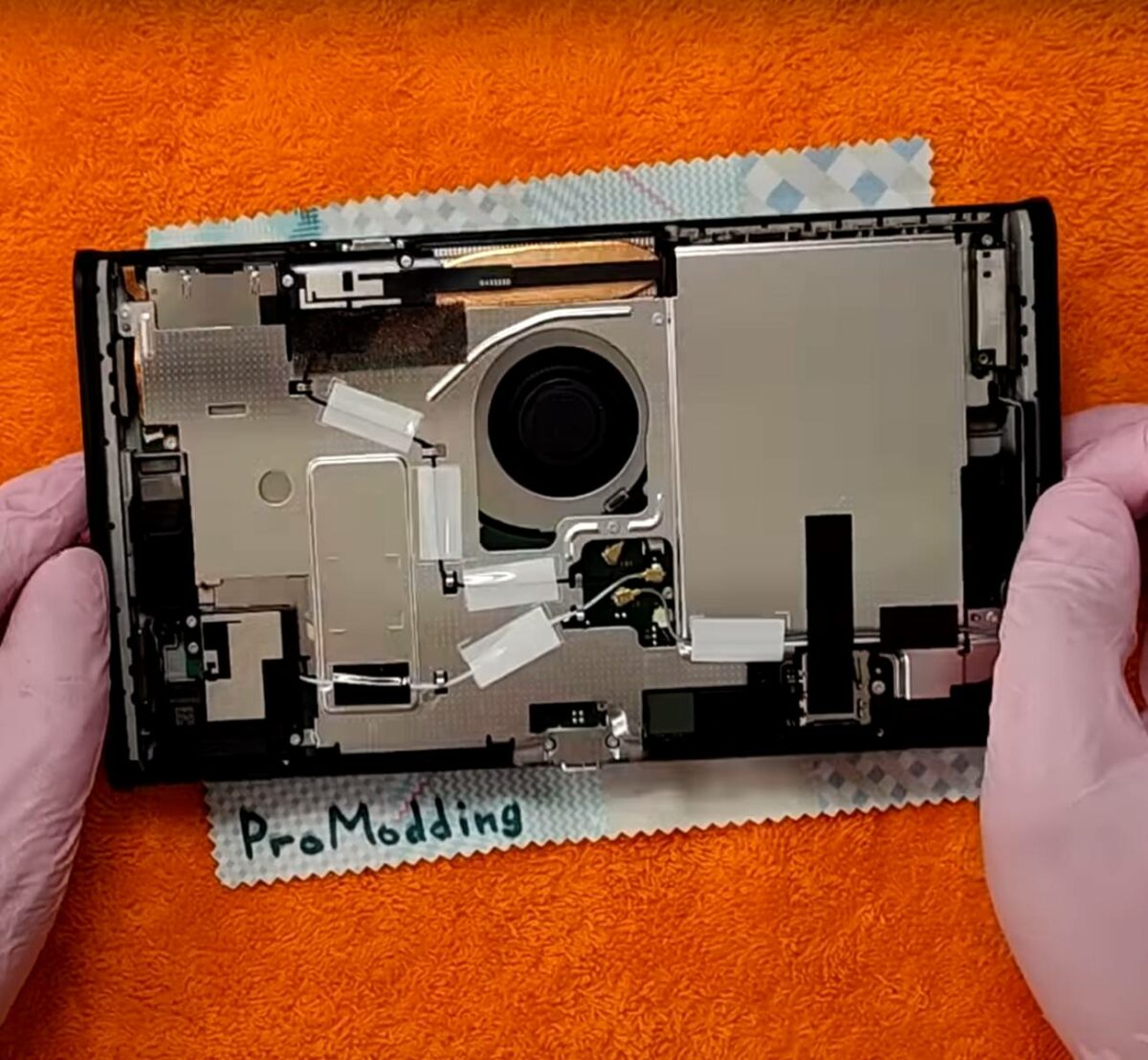
The much-awaited Nintendo Switch 2 console has been dressed down to its knickers, giving us a look at its internal components, centred around a custom Nvidia SoC (System on Chip). Though the handheld is already quite compact, its components take even less room, with about half the space dedicated to cooling and battery.
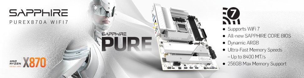
Instead of launching a game or two to enjoy the freshly unboxed console, ProModding went straight for the screwdriver and started disassembling the brand-new Switch 2. Straight away, the YouTuber had to fight the coloured side covers which hide the magnets that secure Joy-Cons 2 in place. It’s a delicate task that takes finesse if you want to put the coloured stickers back, otherwise you can simply tear them and call it a day.
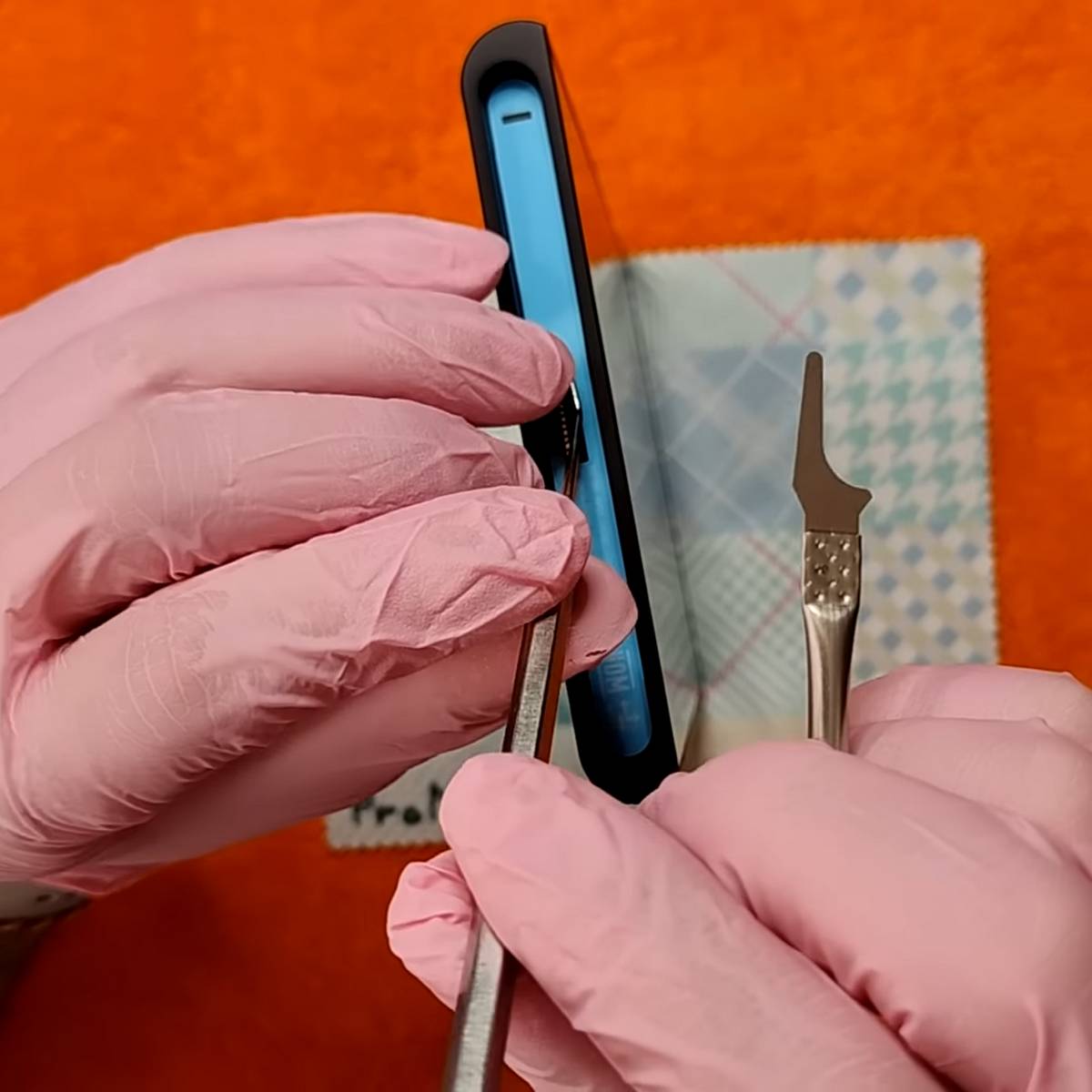
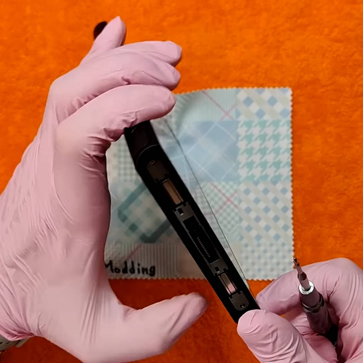
Beneath the stickers lie two screws on each side designed to lock the plastic in place. After removing these, it was only a matter of prying the plastic open without breaking it, which is not as simple as it may sound without an existing teardown guide to walk you through the process. A dozen or so screws later and the console-wide shielding pulls back, giving us our first glance at the motherboard and the heart of the machine.
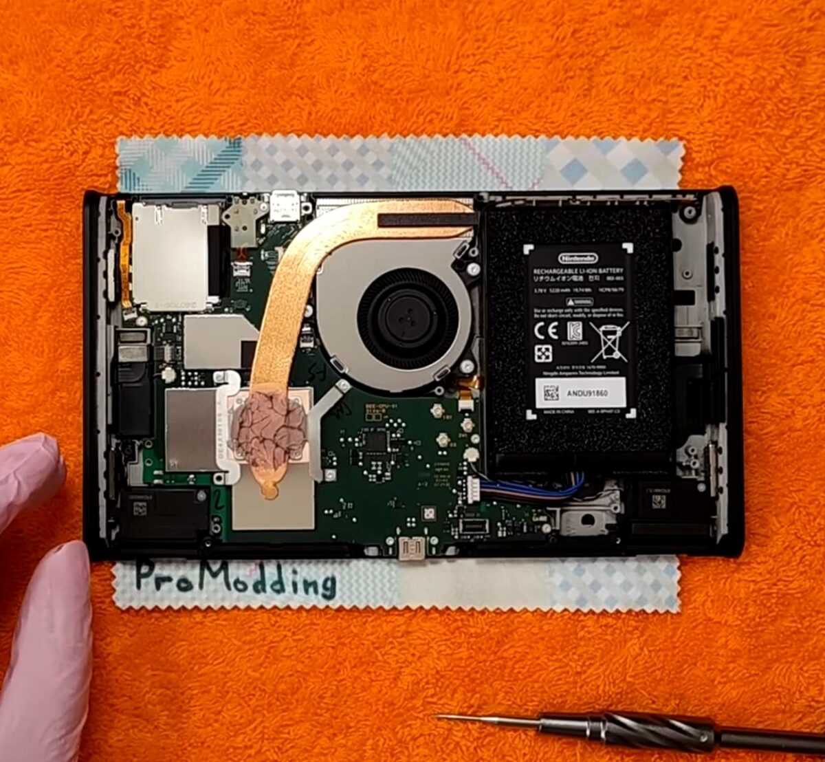
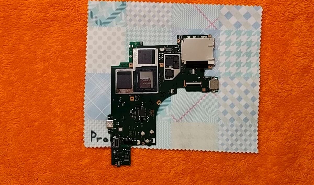
With all the support components away, the motherboard, SoC, RAM, storage, and other power-related parts only took about half the space available inside the Switch 2’s frame. The other half is reserved for the battery pack and fan/cooler assembly. It will always astound me that such a tiny board can facilitate so much fun.
The SoC is undoubtedly the one doing the heavy lifting, custom-made by Nvidia for the Switch 2. It boasts eight ARM Cortex A78C cores sharing 4MB of L3 cache, six of which are available for games while two are reserved for system operations. The same goes for RAM, where 9GB is available to games and 3GB is dedicated to the OS. Lastly, the GPU portion of the SoC packs 1,536 CUDA cores, based on Nvidia’s Ampere architecture.
Overall, the disassembly procedure looked quite tedious, though mainly due to the difficult stickers and layers of shielding. Other than that, there were no obnoxiously glued components or screens getting in the way like they do on smartphones. That said, this task is better left to professionals, at least if you care about getting your console in working order. Now, all that is left is to wait for iFixit to rate the Switch 2’s reparability.