

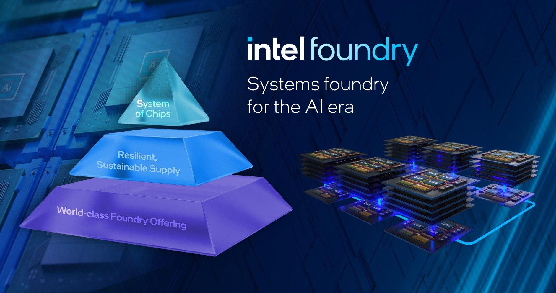
Intel today announced an important reorganisation of its manufacturing business to better meet the needs of myriad customers seeking leading-edge silicon. Known as Intel Foundry, it’s dubbed as the ‘system foundry for the AI era.’
Intel Foundry becomes the overarching umbrella for the current manufacturing side of the company that today encompasses Intel Foundry Services (IFS), Technology Development, and Operational Supply Chain, currently headed by Stu Pann, Ann Kelleher, and Keyvan Esfarjani, respectively. They will continue to serve in present roles.
To be clear, the purpose of Intel Foundry is to serve the eclectic needs of companies requiring cutting-edge silicon for complex manufacturing and packaging of hardware most prominently destined for the burgeoning AI era. A key point worth stressing is that Intel’s own design teams for products such as Xeon, Core, and a phalanx of AI-specific hardware are also seen as a customer for Intel Foundry. In essence, they will compete against third-party fabless companies for a share of the Intel Foundry business, leading to, one would imagine, greater intra-company transparency when apportioning cost and revenue.
Open to all customers
Intel has significant expertise in manufacturing silicon that goes back 50 years. Up until now, the vast majority of silicon turned by out Intel’s fabrication plants has been used to build the company’s own wide portfolio of chips. This ratio of internal vs. external customers looks set to change with the remit imposed upon Intel Foundry.
Announced at an all-new event called IFS Direct Connect, company boss, Pat Gelsinger, said: “AI is profoundly transforming the world and how we think about technology and the silicon that powers it. This is creating an unprecedented opportunity for the world’s most innovative chip designers and for Intel Foundry, the world’s first systems foundry for the AI era. Together, we can create new markets and revolutionize how the world uses technology to improve people’s lives.”
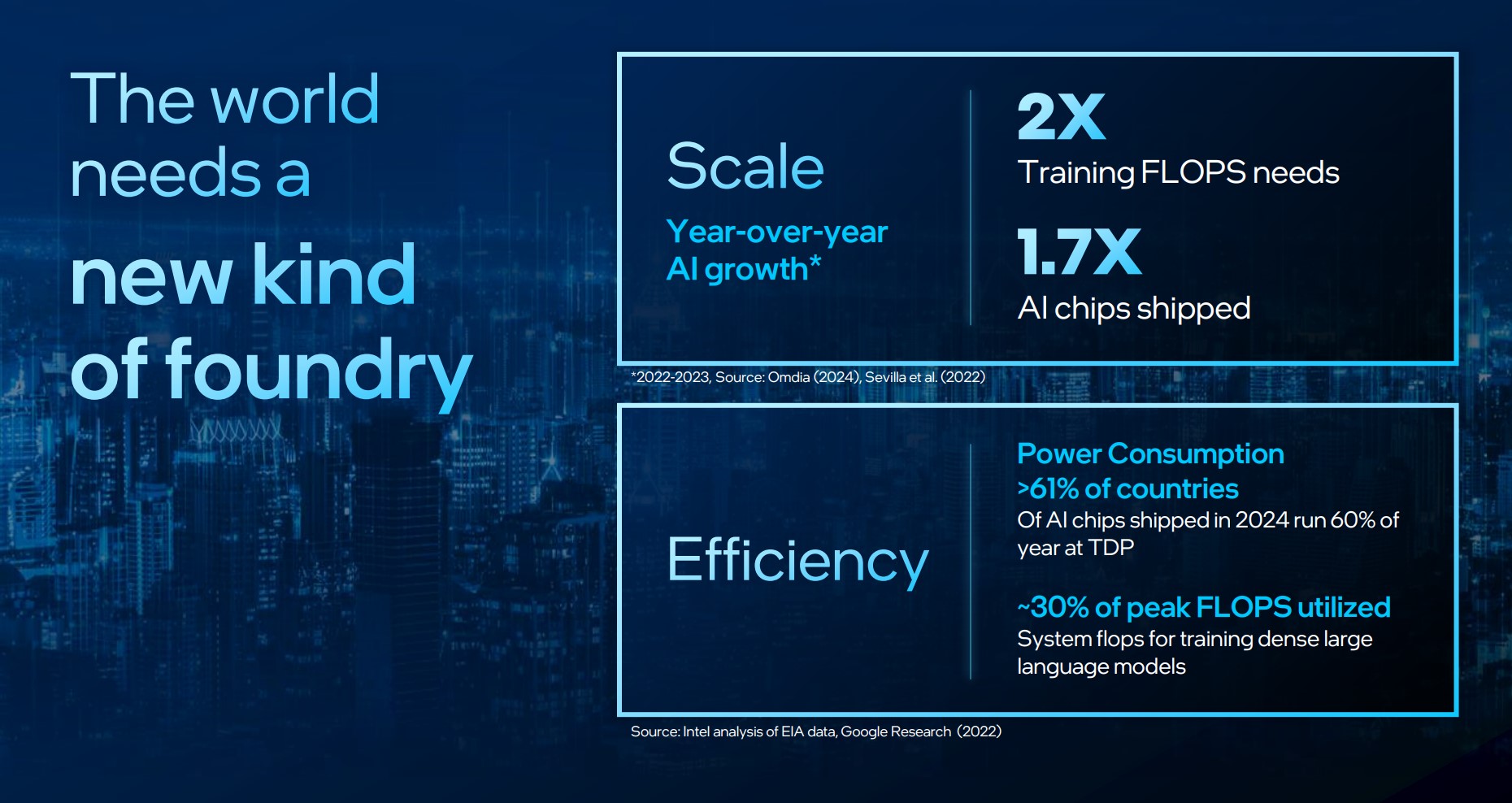
Digging deeper, the current boom in AI chips has led to unprecedented orders that highlight key issues in today’s global manufacturing network. In particular, a combined lack of leading-edge capacity and advanced packaging hinder supply and revenue. This is where Intel trusts its expertise will help alleviate some of the bottleneck.
“We are offering a worldclass foundry, delivered from a resilient, more sustainable and secure source of supply, and complemented by unparalleled systems of chips capabilities. Bringing these strengths together gives customers everything they need to engineer and deliver solutions for the most demanding applications,” said Stu Pann, senior vice president of Intel Foundry.
The backbone of manufacturing at-scale AI
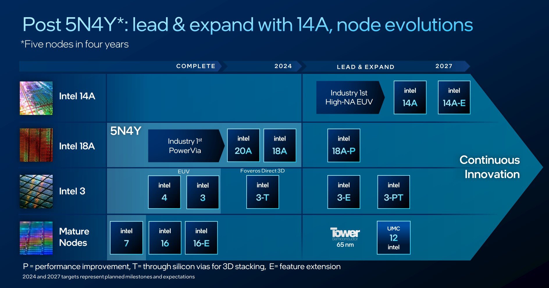
The latest process roadmap speaks to building out AI chips on the most efficient silicon. Known as five nodes in four years (5N4Y), the company announced today that the Intel 3 process is ready for high-volume manufacturing, while next-generation 20A and 18A are on track. Foundry customers can start designs today, with full product designs available in Q2, on 18A, according to Intel’s Craig Orr. Furthermore, the Xeon E-Core Clearwater Forest – you know, the one with up to 288 cores – has already taped out.
Intel expects the next generation of AI systems to use a combination of Compute Dies built on 18A with the Base Die on the marginally cheaper 3 process.
Ambitious manufacturing roadmap
But let’s be clear. The roadmap is ambitious in its scope. Right now, the latest architecture, known as Meteor Lake, is fabricated on the Intel 4 process, so there’s a lot on the right-hand side that remains in the future. Different strains of silicon can be massaged with different characteristics that lend themselves to certain types of products. Some need frequency, others some form of stacking, whilst many benefit from the best-possible efficiency. Look again at the roadmap. You’ll notice certain processes suffixed with certain letters, which is new. There’s E, P, PT, and T.
Answering the clarion call for disparate products built by a foundry, Intel announces feature extension (E) that typically offer less than a five percent performance improvement over the standard silicon. P, meanwhile, is a small step-change in performance on the same node, offering up to 10 per cent, which is useful for high-performance products that insist on bleeding-edge performance. Last but not least, the T denotes silicon ready for some form of 3D-stacking technology. In short, the more the options available, the more of the potential market one can cover.
As an aside, Intel believes it will regain process-node leadership from TSMC and Samsung by the time that the 20A and 18A processes are commercialised later this year.
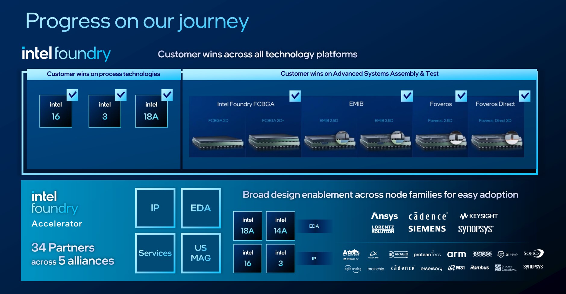
Coming back to the Foundry, Intel has already announced four large-scale customers for the 18A process in 2023. Today, though no names were given, which is normal for this business, further design wins were announced for the Intel 3, 18A and the more mature 16 processes. Knowing Intel’s expertise in packaging through technologies such as EMIB and Foveros, it is reasonable to assume they are a large part in the adoption of Intel Foundry as the manufacturing partner.
Intel today mentioned that 75% of Foundry customer test chips are on the leading 18A process. One of the highest-profile collaborations is Arm, who last year announced a partnership to ensure the process is a viable source for building Arm IP upon. It’s no coincidence that Arm boss, Rene Haas, is a notable speaker at IFS Direct Connect today.
Bullish sentiments
Right now, Intel is naturally bullish on its efforts at becoming a leading foundry partner for the semiconductor industry. The plans are ambitious, actually, with the stated aim to become the number two external foundry by 2030, behind TSMC but ahead of Samsung.
For me, the most interesting aspect is the nuanced shift in Intel’s thinking. Its own product design groups no longer have free rein on manufacturing. Instead, it appears they will need to prove the need for leading-edge capacity, thus competing with external companies for a share of the expensive manufacturing pie. Going by Intel’s missives at IFS Direct Connect, it’s possible upcoming Xeon and Core products may lose out capacity to, say, a fabless partner offering higher revenue-earning opportunity on a particular node. On a pure conjecture front, wouldn’t it be something if future Nvidia products were built by Intel while, at the same time, Xeon and Gaudi had to use TSMC’s know-how?