
Nvidia just unveiled its latest Blackwell GPU architecture, and it already claims it’s the “world’s most powerful chip.” On paper, it certainly looks promising. Manufactured using a custom-built 4NP TSMC process node, this bad boy packs 208 billion transistors, making it Nvidia’s most dense GPU to date. For those keeping score, its predecessor, the H100, has 80 billion transistors.
Team Green achieved this by combining two-reticle limit GPU dies connected via a 10TB/s chip-to-chip link into a single, unified GPU. It’s a monster-sized chip and the first Nvidia GPU that utilises a multi-chip module (MCM) chiplet design. We expect it’ll directly compete with AMD’s upcoming Instinct MI300 architecture.
Unlike previous monolithic designs that use a single large chip, this chiplet approach allows for more efficient production and can potentially increase yields during the manufacturing process. Nvidia claims Blackwell will allow organisations to build and run real-time generative AI on trillion-parameter large language models (LLMs) at up to 25x less cost and energy consumption than its predecessor.
In addition, Blackwell is equipped with the world’s fastest HBM3e memory from Micron. It offers up to 192GB capacity at 8TB/s bandwidth. It’s far more powerful than the rumoured GDDR7 VRAM claim, although that could arrive in future Nvidia GeForce RTX 50 Series card updates.
Alas, we’re getting ahead of ourselves. This immense transistor count indicates Nvidia’s ambition to significantly increase computing capabilities particularly in the AI and HPC territory.
The architecture features no less than six transformative technologies designed for accelerated computing. Nvidia says this will unlock breakthroughs in “data processing, engineering simulation, electronic design automation, computer-aided drug design, quantum computing and generative AI,” which are all emerging fields where the brand sees big cash flow opportunities.
A monster Superchip
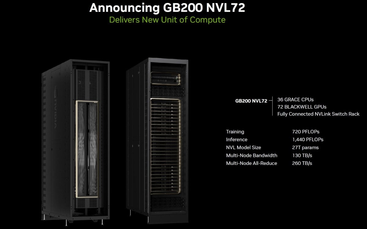
What’s more interesting than a super-powered Blackwell GPU? Well, two of them connected together. Nvidia’s GB200 Grace Blackwell Superchip connects two B200 Tensor Core GPUs to an Nvidia Grace CPU. Thanks to a 900GB/s ultra-low-power NVLink chip-to-chip interconnect.
In fact, Nvidia’s fifth generation NVlink can provide up to 1.8TB/s of full bidirectional bandwidth between up to 576 GPUs. It’s ideal for the most complex LLMs. Combining these two technologies is a key component of the Nvidia GB200 NVL72 – a multi-node, liquid-cooled, rack-scale system for the most compute-intensive workloads. It combines a whopping 36 Grace Blackwell Superchips, consisting of 72 Blackwell GPUs and 36 Grace GPUs.
Nvidia says that the platform will act as a single GPU capable of 1.4 exaflops of AI performance and 30TB of fast memory. It’s also a building block of the DGX SuperPOD: a next-generation AI infrastructure designed for enterprise deployments.
Blackwell-based products will be available from partners starting later this year. This includes Amazon Web Services, Dell Technologies, Google, Meta, Microsoft, OpenAI, Oracle, Tesla, and xAI, to name but a few.